Topic 1: key concepts and revision Flashcards
(21 cards)
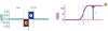
1
Q
Describe the fermi dirac distribution using a sketch to support your answer
A
- The fermi dirac distribution takes the form f(E) = 1 / e(E-Ef)/kT + 1 and describes all available states in a material and whether they are occupied at a given temperature (not whether they are allowed or not)
- For a metal at 0K electrons populate energy levels up to the Fermi energy, Ef
- When T > 0K Ef is the probability of occupancy at 0.5
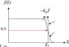
2
Q
- Why does the graph shape change at finite temperature?
A
- As temperature increases higher energy state become occupied
- Therefore, states below Ef have less chance of being occupied
3
Q
What is a hole in term of electronics?
A
- Used to describe properties of a vacant electron state in an otherwise full band
4
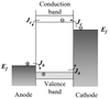
Q
- How do energy levels differ in semiconductors compared with metals?
A
- In a metal, the conduction band (CB) ? is partially occupied up the fermi level
- In semi-conductors the fermi level lays between the fully occupied valence band (VB) and the first unoccupied band, the conduction band (CB) in an energy gap
5
Q
- What is the vacuum level?
A
- Area outside of solid surface/molecule where electron is free
- Make sure to draw this on diagrams as well as energy on y axis
6
Q
- Define conductivity
A
- σ =J/E where J is current density and E is electric field
7
Q
- Define conductivity in terms of electrons/holes
A
- σ =nppµp + neeµe
- np/e -desnity of holes/electrons
- p/h – charge on a hole/electron (+/- 1.6E-19 C)
- µp/n – hole/electron mobility (cm2 V-1 s-1)
8
Q
Graphene is a semiconductor, but equally as conductive as many metals, why is this?
A
- Graphene has a low density of electrons but very large mobility
- Metals are the opposite to this
9
Q
- How can hole/electron density be increased?
A
Doping; incorporate impurity states in to lattice that can pull electrons out of VB – hole/ inject electrons in to CB – electrons
10
Q
- How does the size of materials affect its properties?
A
- As a material is shrunk down, the proportion of atoms at the surface becomes more significant due to an increase in SA/V ratio
- Leads surfaced environment properties to dominate functionality of device more.
- And example of a structure that uses this would be carbon nanotubes
11
Q
- What is charge transfer doping and what are its advantages over conventional doping?
A
- Molecular adsorption of a molecule on to a surface where charge transfer occurs at the frontier molecular orbitals between the two species
- This does not disrupt the lattice, therefore not degrading the mobility as we have no need to break any bonds to introduce an impurity.
12
Q
- Why is conductance (G) used in nanotechnology rather than conductivity (σ)?
A
- G = IV is a measure of ease of flow of current along a given path (i.e. through a specific component)
13
Q
- G is only … under very specific conditions, when transport is … ,
- Meaning there is no … of electrons that move through material
A
- G is only quantized under very specific conditions, when transport is ballistic,
- Meaning there is no scattering of electrons that move through material
14
Q
- Describe and explain the following graph
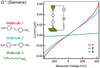
A
- Gradient near x/y axis gives conductance of each molecule (G = I/V)
- This would indicate molecule ½ are highly conjugated and 3 is saturated as expected
- The amount of current for a given voltage is much higher due to delocalised p orbitals.
15
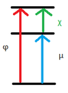
Q
- What is the work function (ϕ)?
A
- The energy required to eject an electron from the fermi level up and out to the vacuum level.
16
Q
- How can the came material have a different number of work functions?
A
- Work function will be different depending on which crystal face is exposed (i.e. Ag 100 WF will differ from 111 due to a different arrangement of atom sat the surface)
17
Q
- Describe the components of the work function
A
- Chemical potential (µ) – associated with atom type
- Surface potential (χ) – depends on crystal face/ arrangement of atoms on surface.
18
Q
Explain how does the surface potential (SP) affects the WF
A
- Electron density has a probability to spill outside of solid at finite temperature
- This causes a dipolar layer to form at the interface that an ejectin electron must travel through.
- This causes an increase in potential energy.
19
Q
- What is the pushback/pillow effect?
A
- An absorbed molecule (even only weakly physisorbed) can push electrons spilling into the vacuum back in to the solid
- Coulombic repulsion and Pauli exclusion between electron densities of adsorbate and surface lead to compression of metal surface dipole tail by adsorbate.
- However, this is not a charge transfer process

20
Q
Describe the charge transfer interaction of chemisorbed surface adsorbates and how it affects the work function
A
- Change in WF not due to push back effect
- Ionisation voltage is less than the metal WF in donor adsorption from high energy HOMO
- Reverse is true for acceptors, with charge transfer to low energy LUMO

21
Q
- Complexity at …-…interfaces makes is difficult to predict extent of … between Ef in metal and … molecular orbitals when charge transfer due to adsorbate moves the fermi level of the metal, making prediction difficult.
A
- Complexity at metal-organic interfaces makes is difficult to predict extent of alignment between Ef in metal and frontier molecular orbitals when charge transfer due to adsorbate moves the fermi level of the metal, making prediction difficult.
