Photonics Exam Deck Flashcards
(37 cards)
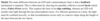
Topic 2: The real and imaginary parts of the complex relative permittivity of a material at a wavelength of 0.65 µm are 19.72 and 2.56, respectively. Find the complex refractive index. What is the power loss coefficient?


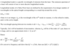
Topic 2: Snell’s Law and evanescent wave form

Note how the equation for cosθt s changed with the deduction that the square root will be negative knowing that the incidence angle is greater than the critical angle.
Also note how the propagation constant can take more than direction. Direction of oscillation of the e-field, y, is zero in this case.

Topic 3: Could Al0.5Ga0.5As be used for the active layer of an LED? Give your reasons.
No – this composition of AlGaAs does not have a direct bandgap, since x > 0.43.
Topic 3: . What are the advantages of using a quaternary alloy such as InGaAsP?
The InGaAsP system allows alloys with a wide range of compositions and a wide range of bandgap energies to be grown. Using a quaternary alloy allows independent control of 𝐸𝑔 and the lattice constant (making it possible to lattice match to InP substrates, for instance).
Topic 4: What are the essential conditions for lasing to occur?
For lasing, we need gain and feedback. Gain is obtained when there is net stimulated emission, which requires population inversion. Feedback can be provided by, for example, placing the gain medium in a Fabry-Perot etalon
Topic 4:
(a) If the laser in the previous question operates at a wavelength of 1300 nm, find the number of wavelengths in a round trip of the cavity (i.e. find the integer ). Assume a refractive index of 3.5.
(b) What is the longitudinal mode spacing in nm?
Do b) - what do you need to remember?
Differentiate f = c/𝜆

Topic 4: The threshold current of a semiconductor laser is 20 mA and its slope efficiency is 0.3 W.A-1 . What is the output power at a drive current of 70 mA?
The output power will be approximately zero at the threshold drive current, then will increase linearly with the additional current above threshold, with the slope give by the slope efficiency. Drive current of 70 mA is 50 mA above threshold, so the output power at 70 mA will be 70 × 0.3 = 𝟐𝟏 mW.
Topic 4: The lecture notes show the LI plots for a laser at 0, 25 and 50 C. Estimate the characteristic temperature of this laser.
Estimating the threshold currents at 0°C and 50°C to be 47 mA and 62 mA respectively, we can find 𝑇0 as follows:
Using a rearranged form of the attached equation (with T1 an T2 representing the threshold currents).
𝑇0 = (50 − 0) / ln ( 62 / 47) = 𝟏𝟖𝟎 K

Topic 4: Explain why a three-level system is required to achieve population inversion in an optically pumped solid-state laser. What additional advantage is provided by using a four-level system?
- 2 level system
- for rate of absorption from level 1 to level 2 and rate of stimulated emission from level 2 to level 1, the Einstein B coefficients are the same
- processes are equally likely, prevent 𝑁2 becoming greater than 𝑁1
- not actually possible to achieve population inversion
- 3 level system
- pumping occurs to a higher energy state E3, from which the particles rapidly decay to a relatively long-lived (metastable) state E2
- population inversion can be achieved between E2 and E1
- Problem:
- takes time to achieve the population inversion – at least half the particles originally in state E1 must be pumped to E2 via E3
- Thus lasing cannot begin immediately once pumping starts.
- 4-level system
- Avoids problem of 3-level system,
- pumping from a ground state E0 which has a lower energy than E1.
- If E1 is initially nearly empty, then as soon as particles are pumped to E2 via E3, population inversion is achieved and lasing can occur.
- To maintain population inversion, particles in energy state E1 need to rapidly decay back to the ground state E0
- So that the number of particles in E1 is kept low
- Avoids problem of 3-level system,
Topic 4: Using diagrams, explain the main differences between an LED and a semiconductor laser in terms of (a) their light-current characteristics, and (b) their output spectra.
- (a)
- The light output from an LED is just due to spontaneous emission, so will increase approximately linearly with drive current (but probably curving slightly down, particularly at high drive currents).
- Lasers emit spontaneous photons below threshold, but once the threshold current is reached, stimulated emission dominates, and the light output increases linearly from the threshold current.
- (b)
- The spectrum of an LED will be quite broad (maybe 20 nm full-width at half maximum), because spontaneous emission can occur from a range of energies in the conduction band (and, to a lesser extent, to a range of energies in the valence band).
- Lasers (specifically Fabry-Perot lasers) will emit in one or a few narrow spectral lines. Although stimulated emission can occur at a range of wavelengths, due to the distribution of energy states within the conduction and valence bands (so similar to the range of spontaneous emission in an LED), the lasing threshold will be reached first close to the peak emission wavelength, and once reached, the carrier density will be clamped, preventing other modes from reaching threshold. Thus, only one longitudinal cavity mode (corresponding to the round-trip gain and phase conditions being met) should lase.
- In practice, the carrier density may not be completely clamped above threshold, allowing other modes to lase.

Topic 4: What do you need to remember about applying the power conversion efficiency equation to semiconductor lasers?
They might ive you the output power but you need to remember that there are two facets, and both facets give the same output.
Thus output power in the PCE equation should be 2x
Topic 4: A buried heterostructure semiconductor laser emitting at a wavelength of 1550 nm is 400 µm long and has a waveguide cross-section area of 0.3 µm x 1 µm. Both facets have a reflectance of 30%. Find the threshold carrier density if the power loss coefficient, 𝜶, is 20 cm-1 , and the gain coefficient is given by 𝒈(𝑵) = 𝟐 × 𝟏𝟎−𝟏𝟔(𝑵 − 𝟏. 𝟓 × 𝟏𝟎𝟏𝟖) cm-1 (where 𝑵 is the number of carriers per cm3 ). Estimate the photon density in the laser cavity when the output power Drive Threshold current Output Power Laser LED Wavelength Output Power Laser LED from each facet is 5 mW (assume a refractive index of 3.5). How many photons are there in the laser cavity?

Topic 4: A 1.55 µm laser with a cavity length of 600 µm lases with a multi-longitudinal-mode spectrum with full width at half maximum (FWHM) of 2 nm. Estimate the number of cavity modes in the laser spectrum. (Assume a refractive index of 3.5.)
The mode spacing in frequency is Δ𝑓 = 𝑐/(2𝑛𝐿) = 71.4 GHz = 0.57 nm (1 nm = 125 GHz at 𝜆 = 1.55 µm). Assuming a roughly triangular spectrum, the total width is 4 nm. So there are approximately 4/0.57 = 7 lasing modes
Topic 4: Explain the advantages of index guiding (as in a buried heterostructure laser) over gain guiding (as in a simple stripe contact laser).
- In a buried heterostructure, the stripe of active material is surrounded on all sides by lower refractive index material, forming a dielectric waveguide. The index guiding ensures the light is tightly confined in the active material, and that the mode distribution doesn’t change as the drive current is varied. The buried heterostructure also has a well-defined active region, through which the injected current flows uniformly. Altogether, these factors result in lower threshold current and higher slope efficiency, and enable stable emission to higher output powers.
- In a gain guided laser, the active region width depends on the area through which the current flows, since this is where there will be optical gain (hence gain guiding). The current spreads out below the strip contact, meaning that the gain region under the stripe is wider than the stripe, and the current density varies laterally under the stripe, so the active region width is not very well defined. As a result, the threshold current will be higher than would be calculated based on the stripe width, and efficiency is lower. The carriers injected into the gain region cause a small change in refractive index, which provides some weak index guiding, but this will vary with drive current, which can lead to instability in the operation of the laser.
Topic 6: A semiconductor heterostructure waveguide has 𝒏𝟏 = 3.50 and 𝒏𝟐 = 𝟑. 𝟒𝟗. What is the maximum waveguide width for single-mode operation at a wavelength of 0.85 µm?

Topic 6: By considering the graphical method of solving for the modes of the symmetrical slab waveguide, estimate the number of modes in terms of the V parameter. Hence estimate the number of modes that can be supported by a 50 µm wide slab waveguide with 𝒏𝟏 = 𝟏. 𝟒𝟓𝟎 and 𝒏𝟐 = 1.435 at a wavelength of 1 µm.

Topic 7: What is the bit period for a 6.25 Gb/s OOK RZ signal? If the pulse width is 𝑻𝒃/𝟒, at what frequency from the carrier is the first null in the spectrum?
𝑇𝑏 = 1/𝑅𝑏 = 160 ps. Pulse width = 40 ps. First null in spectrum is at 1/(pulse width) = 25 GHz.
Topic 7: Calculate the loss and output power after 100 km of standard fibre at wavelengths of 1.55 µm and 1.3 µm. Assume Pin= 5 mW.
5 mW = 7 dBm.
At 1.55 μm, loss = 0.2 dB/km x 100 km = 20 dB; output power = -13 dBm (0.05 mW).
At 1.3 μm, loss = 0.5 dB/km x 100 km = 50 dB; output power = -43 dBm (0.05 μW).
Topic 7: A 10 Gb/s optical communications system operates at a wavelength of 1.55 µm. Estimate the width of a pulse representing an isolated binary “1” after 100 km of standard fibre if raised cosine pulse shaping with 𝜶 = 0.8 is used.
Assume the bandwidth of the signal is limited to 20 GHz (i.e. the central lobe of the spectrum).
At 1.55 μm, 1 nm = 125 nm, so Δ𝜆 = 20/125 = 0.16 nm.
Δ𝑡 = 𝐿. Δ𝜆.𝐷 =100 x 0.16 x 17 = 272 ps. Assuming this spreading adds to the original pulse, the pulse width after 100 km is 372 ps.
Topic 7: Look over the rest of the questions!

Explain the terms direct and indirect bandgap semiconductor with the aid of diagrams. Which type Should be used ‘as the active region of a light-emitting diode (LED)? State the reasons for your answer.
In a direct band gap semiconductor, the top of the valence band and the bottom of the conduction band occur at the same value of momentum.
In an indirect band gap semiconductor, the maximum energy of the valence band occurs at a different value of momentum to the minimum in the conduction band energy.

An LED is fabricated from the semiconductor layer structure illustrated in Figure 1.1:
b) The LED will emit light close to the bandgap wavelength of GaAs, i.e. at about 870 nm.
c) The advantages are: good carrier confinement; high injection efficiency; no re-absorption losses in AlGaAs; produces a guided wave structure because refractive index of AlGaAs is less than that of GaAs.

Define the terms internal and external quantum efficiency for light generation in a semiconductor p-n junction. What factors determine each of these efficiencies?
- The internal quantum efficiency is the ratio of the radiative recombination rate to the sum of the radiative and non-radiative recombination rates.
- Depends on the radiative and non-radiative carrier lifetimes
- Determined by factors such as:
- is material direct or indirect bandgap,
- carrier injection level
- doping concentration
- impurity concentration
- crystal defects (e.g. at hetero-interfaces).
- Determined by factors such as:
- Depends on the radiative and non-radiative carrier lifetimes
- The external quantum efficiency is the ratio of the number of photons emitted to the number of carriers crossing the junction.
- Depends on internal quantum efficiency,
- Depends on factors that determine whether the generated photons are absorbed before they are emitted (e.g. half will be lost into substrate, absorption in capping layers, reflection from semiconductor-air interface, total internal reflection at some angles).
With the aid of a schematic diagram, briefly describe the three main band-to-band electronic transitions that you might expect to occur in a simple two-level energy system. Your schematics should clearly indicate which processes require an incoming radiation wave.
- a)
- Absorption of photons, where a photon excites a system from a lower energy state (𝐸1 in the diagram) to a higher energy state (𝐸2), e.g. a photon excites an electron from the valence band to the conduction band in a semiconductor.
- b)
- Spontaneous emission, where a system moves randomly from a higher to a lower energy state (i.e. 𝐸2 to 𝐸1 in the diagram), giving off a photon in the process (an example is an EHP recombining in a semiconductor).
- c)
- stimulated emission, involves an incoming photon causing (stimulating) a system in a higher energy state to lose energy and give off a new photon, without the original photon being absorbed. Photon generated in this stimulated emission process is identical to the incoming photon, that is, it has the same frequency (energy), phase, and direction as the incoming photon.